

เข้าสู่ระบบ เข้าร่วมฟรี


1 / 3
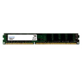
ข้อมูลจำเพาะของโมดูลหน่วยความจำ DDR3 UDIMM
| Model No. : | NSO4GU3AB |
|---|
Huizhou, Guangdong, China
- ผู้ผลิต
- บริษัท การค้า
- ซัพพลายเออร์ทองคำ

- การรับรองแพลตฟอร์ม

- งานแสดงสินค้าออนไลน์


รายละเอียดสินค้า
4GB 1600MHz 240 พิน DDR3 UDIMM
ประวัติการแก้ไข
|
Revision No. |
History |
Draft Date |
Remark |
|
1.0 |
Initial Release |
Apr. 2022 |
|
![]()
ตารางข้อมูลการสั่งซื้อ
|
Model |
Density |
Speed |
Organization |
Component Composition |
|
NS04GU3AB |
4GB |
1600MHz |
512Mx64bit |
DDR3 256Mx8 *16 |
คำอธิบาย
Hengstar Unbuffered DDR3 SDRAM DIMMS (โมดูลข้อมูลสองเท่าที่ไม่ได้รับการบัฟเฟอร์แบบซิงโครนัส DRAM โมดูลหน่วยความจำแบบอินไลน์คู่) มีพลังงานต่ำโมดูลหน่วยความจำการทำงานความเร็วสูงที่ใช้อุปกรณ์ DDR3 SDRAM NS04GU3AB เป็น 512M x 64- บิตสองอันดับ 4GB DDR3-1600 CL11 1.5V SDRAM ผลิตภัณฑ์ DIMM ที่ไม่ได้รับการบัฟเฟอร์ซึ่งใช้ส่วนประกอบ FBGA 256M 256M x 8-bit SPD ถูกตั้งโปรแกรมให้กับเวลาแฝงมาตรฐาน DDR3-1600 ของ JEDEC ที่ 11-11-11 ที่ 1.5V DIMM 240 พินแต่ละอันใช้นิ้วสัมผัสทองคำ SDRAM Unbuffered DIMM มีไว้สำหรับใช้เป็นหน่วยความจำหลักเมื่อติดตั้งในระบบเช่นพีซีและเวิร์กสเตชัน
คุณสมบัติ
Power Supply: VDD = 1.5V (1.425V ถึง 1.575V)
VDDQ = 1.5V (1.425V ถึง 1.575V)
800MHz FCK สำหรับ 1600MB/วินาที/พิน
8ธนาคารภายในอิสระ
Latency CAS ที่ตั้งโปรแกรมได้: 11, 10, 9, 8, 7, 6
latency Additive Additive Latency: 0, Cl - 2 หรือ Cl - 1 นาฬิกา
8บิตล่วงหน้า
ความยาวเบิร์สต์: 8 (interleave โดยไม่มีขีด จำกัด ใด ๆ ตามลำดับที่อยู่ที่อยู่เริ่มต้น“ 000” เท่านั้น), 4 กับ TCCD = 4 ซึ่งไม่อนุญาตให้อ่านหรือเขียนได้อย่างไร้รอยต่อ [ไม่ว่าจะโดยใช้ A12 หรือ MRS]
data data data data data
การสอบเทียบ (ตนเอง) การสอบเทียบตนเองภายในผ่าน ZQ PIN (RZQ: 240 OHM ± 1%)
การเลิกตายโดยใช้ PIN ODT
ช่วงเวลาการรีเฟรชค่าเฉลี่ย 7.8US ที่ต่ำกว่า TCASE 85 ° C, 3.9US ที่ 85 ° C <TCASE <95 ° C
การรีเซ็ต asynchronous
ความแข็งแรงของไดรฟ์ข้อมูลที่ปรับได้ไม่ได้
topology
PCB: ความสูง 1.18” (30 มม.)
Rohs เป็นไปตามข้อกำหนดและปราศจากฮาโลเจน
พารามิเตอร์เวลาที่สำคัญ
|
MT/s |
tRCD(ns) |
tRP(ns) |
tRC(ns) |
CL-tRCD-tRP |
|
DDR3-1600 |
13.125 |
13.125 |
48.125 |
2011/11/11 |
ตารางที่อยู่
|
Configuration |
Refresh count |
Row address |
Device bank address |
Device configuration |
Column Address |
Module rank address |
|
4GB |
8K |
32K A[14:0] |
8 BA[2:0] |
2Gb (256 Meg x 8) |
1K A[9:0] |
2 S#[1:0] |
คำอธิบายพิน
|
Symbol |
Type |
Description |
|
Ax |
Input |
Address inputs: Provide the row address for ACTIVE commands, and the column |
|
BAx |
Input |
Bank address inputs: Define the device bank to which an ACTIVE, READ, WRITE, or |
|
CKx, |
Input |
Clock: Differential clock inputs. All control, command, and address input signals are |
|
CKEx |
Input |
Clock enable: Enables (registered HIGH) and disables (registered LOW) internal circuitry |
|
DMx |
Input |
Data mask (x8 devices only): DM is an input mask signal for write data. Input data is |
|
ODTx |
Input |
On-die termination: Enables (registered HIGH) and disables (registered LOW) |
|
Par_In |
Input |
Parity input: Parity bit for Ax, RAS#, CAS#, and WE#. |
|
RAS#, |
Input |
Command inputs: RAS#, CAS#, and WE# (along with S#) define the command being |
|
RESET# |
Input |
Reset: RESET# is an active LOW asychronous input that is connected to each DRAM and |
|
Sx# |
Input |
Chip select: Enables (registered LOW) and disables (registered HIGH) the command |
|
SAx |
Input |
Serial address inputs: Used to configure the temperature sensor/SPD EEPROM address |
|
SCL |
Input |
Serial |
|
CBx |
I/O |
Check bits: Used for system error detection and correction. |
|
DQx |
I/O |
Data input/output: Bidirectional data bus. |
|
DQSx, |
I/O |
Data strobe: Differential data strobes. Output with read data; edge-aligned with read data; |
|
SDA |
I/O |
Serial |
|
TDQSx, |
Output |
Redundant data strobe (x8 devices only): TDQS is enabled/disabled via the LOAD |
|
Err_Out# |
Output (open |
Parity error output: Parity error found on the command and address bus. |
|
EVENT# |
Output (open |
Temperature event: The EVENT# pin is asserted by the temperature sensor when critical |
|
VDD |
Supply |
Power supply: 1.35V (1.283–1.45V) backward-compatible to 1.5V (1.425–1.575V). The |
|
VDDSPD |
Supply |
Temperature sensor/SPD EEPROM power supply: 3.0–3.6V. |
|
VREFCA |
Supply |
Reference voltage: Control, command, and address VDD/2. |
|
VREFDQ |
Supply |
Reference voltage: DQ, DM VDD/2. |
|
VSS |
Supply |
Ground. |
|
VTT |
Supply |
Termination voltage: Used for control, command, and address VDD/2. |
|
NC |
– |
No connect: These pins are not connected on the module. |
|
NF |
– |
No function: These pins are connected within the module, but provide no functionality. |
หมายเหตุ : ตารางคำอธิบายพินด้านล่างเป็นรายการที่ครอบคลุมของพินที่เป็นไปได้ทั้งหมดสำหรับโมดูล DDR3 ทั้งหมด พินทั้งหมดที่ระบุไว้ในพฤษภาคม ไม่ได้รับการสนับสนุนในโมดูลนี้ ดูการกำหนด PIN สำหรับข้อมูลเฉพาะสำหรับโมดูลนี้
ไดอะแกรมบล็อกการทำงาน
4GB, 512MX64 โมดูล (2RANK ของ X8)


ขนาดของโมดูล
มุมมองด้านหน้า

มุมมองด้านหน้า

หมายเหตุ:
1. ขนาดทั้งหมดอยู่ในมิลลิเมตร (นิ้ว); สูงสุด/นาทีหรือทั่วไป (typ) ที่ระบุไว้
2. การยอมรับในทุกมิติ± 0.15 มม. เว้นแต่จะระบุไว้เป็นอย่างอื่น
3. ไดอะแกรมมิติสำหรับการอ้างอิงเท่านั้น


Huizhou, Guangdong, China
- ผู้ผลิต
- บริษัท การค้า
- ซัพพลายเออร์ทองคำ
- การรับรองแพลตฟอร์ม
- งานแสดงสินค้าออนไลน์
ส่งคำถามของคุณไปยังซัพพลายเออร์รายนี้